
Printed circuit boards (PCBs) play a critical role in our increasingly digital world. They’re necessary in powering various electronic devices that we depend on everyday. So given this demand for PCBs, it makes sense to optimise their production. And this starts at the design stage. By fine-tuning the layout and design of PCBs, businesses can achieve lower production costs while maintaining optimal performance. In this article, we’ll delve deeper into the ins-and-outs of PCB layouts, and the benefits of optimising PCB design.
What is a Printed Circuit Board (PCB) Layout?
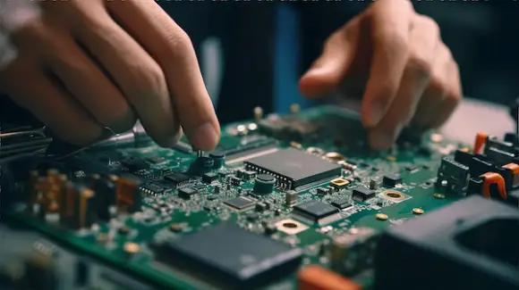
Before we take a closer look at optimisation of printed circuit board layouts, let’s first understand what a PCB, and a PCB layout, are. A printed circuit board is a mechanical support product. It features copper conductors that allow the electrical connections between components that need electricity. In essence, it’s a small, advanced electrical circuit that helps our electronics work.
Before a PCB can be manufactured, it needs to be designed. PCB layout refers to a set of processes used to create a PCB. To make sure that they function as best as they can, PCBs need to be precisely designed. This involves the mechanical structure itself, the fabrication (ie manufacturing) process, as well as the correct placement and insulation of conductive features.
This is achieved through a digital process that allows designers to fine-tune the PCB layout. Designers typically use CAD software in this process. They take into account the electrical requirements of the circuit board, as well as how the file can be prepared for manufacturing. The PCB layout includes traces, mounting hole cutouts, and the placement and routing of wires and components. Once the layout is finalised, the design file is sent to the manufacturer for production.
Why Optimise PCB Layouts?
PCBs and their layouts consist of multiple components and features that need to work together. Given the intricate nature of what is involved, the process can easily eat up production time. However, optimising a PCB layout can significantly streamline the process. And it can do this without compromising quality. And by optimising the PCB layout, businesses can achieve:
- Improved performance – PCBs are more reliable and work more effectively.
- Reduced costs – Optimised PCBs operate more efficiently and in turn have an improved life cycle. This can significantly impact your bottom line in the long run.
- Simplified manufacturability – An optimised PCB means a quality product manufactured at a lower cost. It’s a win-win for everyone.
Best Practices for Optimising PCB Layouts
So we’ve seen that an optimised PCB layout brings a wide range of benefits. But what techniques can be used to optimise PCB layouts? Let’s take a look at some of the most common:
1.Start With a Good Component Library
Every component that is to be mounted onto a PCB has a defined package. A good component library have a set of copper layers and mechanical layers that are suitable for the component package, called a footprint. The copper features, or pads, are designed to mount and connect the component to the interconnecting tracks. Well designed pads will enable quality solder joints, suitable for the end application. The mechanical layers provide documentation or PCB features that aid both manufacture and maintenance. This can include 3D component models providing additional design verification.
2.Utilise Layout Rules
Many component to component, or component to connector, signal types can include specific tracking requirements to achieve reliable operation. Rules can be configured to ensure correct compliance to these requirements, such as meeting length, impedance or clearance to other signals, for example.
3.Manual or Autorouting? A Mixture of Both
Autorouting is a common feature of PCB layout software. It automatically maps out the track (or trace) of the copper wiring, fuses, and insulation on a PCB. It’s this track that connects the components together, and where the electricity will flow. Although this autorouting can be useful, it is not completely reliable. Sometimes, a human touch is needed especially when it comes to sense checking tracks. We recommend manually checking autorouting results and, for straightforward tracks, consider manual routing. This combined approach often results in a more efficient design that performs better in the long term.
4.Keep Trace Lengths Short and Sweet
To improve the performance of the system, it’s best to keep the trace lengths short and direct, where appropriate. Long and complex traces can impact on the system’s performance. Therefore, it’s recommended to keep the traces as direct as possible. This will ensure that your PCBs are working efficiently.
5.Keep In Mind – Where’s It Going To Go?
It’s important to remember that a PCB will be incorporated into a product. To ensure that the installation process is easy, we recommend cooperating with the mechanical designers and verifying 3D suitability throughout the process. Little things like this can mean you won’t have to go back to the PCB layout and reconfigure the design if there’s any problems with getting it to fit.
How DSL Can Help
We offer customised PCB layout services that are tailored to specific project requirements. Our goal is to provide cost-effective and application-specific solutions that are optimised for performance. With years of experience and an extensive component library, we efficiently and effectively design PCBs, all in collaboration with our customers.
We use the latest tools and primarily work with the Altium suite to ensure efficient manufacturability. We understand that the PCB design stage is integral to the success of the PCB. We also take into consideration that they may need to function under extreme temperature conditions. Our qualified engineers undertake PCB design work, and take a ‘right first time’ approach, working to eliminate potential issues that could persist throughout the product’s lifetime. Trust us to deliver the PCB layout that’s bespoke to you.