Power management is a critical aspect of electronic design, as it impacts both the performance and the lifespan of the device. In this blog post, we’ll discuss some best practices for designing a PCB layout that maximizes power efficiency.
What is a PCB Layout?
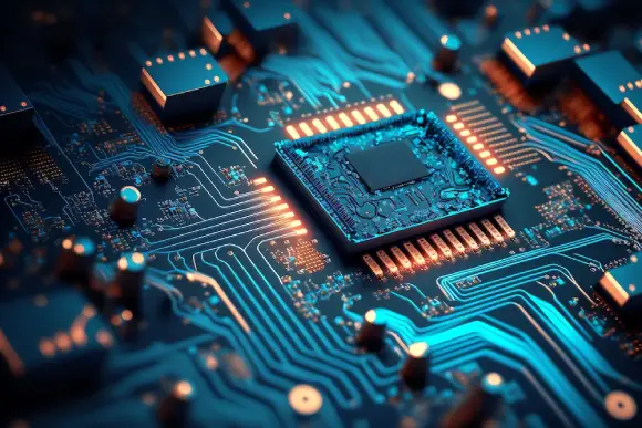
A PCB layout is the physical design of a printed circuit board (PCB), which is the base material for electronic components. It is the process of arranging and connecting the various components, such as transistors, diodes, capacitors, and microcontrollers, on a PCB in a way that ensures the proper functioning of the electronic circuit.
The PCB layout includes the placement of the components, routing of the connections between them (known as traces), as well as the design of the power and ground planes. The layout must take into account the physical size and shape of the components, as well as their electrical characteristics and requirements, such as power and signal integrity.
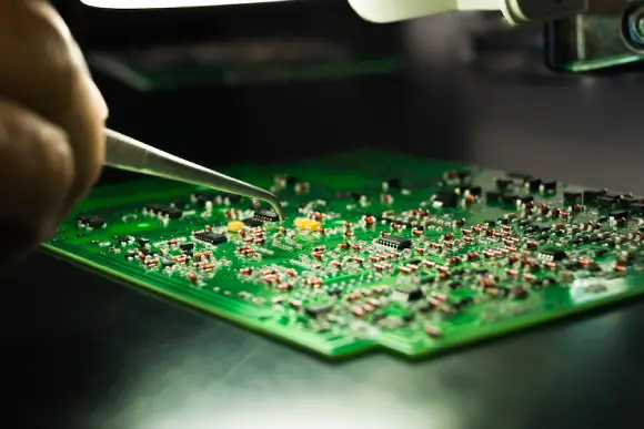
It forms a critical step in the design process, partly as it determines the performance and reliability of the electronic circuit. It is typically done using specialised software which allows the designer to create a virtual representation of the PCB and simulate its performance before it is manufactured.
The layout needs to happen as part of the design, but also needs to be performed in a way to maximise, and certainly no impede, performance and reliability.
The PCB Layout Design Process
The first step in designing a power-efficient PCB layout is to understand the power requirements of the devices. This includes identifying the power sources, the load currents, and the voltage levels.
Once you have a clear understanding of the power requirements, you can start to plan the layout of the PCB.
Generally all switch mode power supplies are kept away from the other circuits and preferably at the power input. The layout needs to ensure that the power available at the devices is sufficient for all needs, under all circumstances. We do this through the trace/plane thicknesses and localised capacitance.
Another important aspect of power management is thermal management.
Thermal Management in PCB Design
Thermal management is the process of controlling and regulating the temperature of electronic devices and systems to ensure their proper functioning and longevity. It is important because electronic components can be sensitive to temperature changes, and high temperatures can cause them to malfunction or fail prematurely.
Thermal management includes both the design and the operation of electronic systems to dissipate heat and prevent overheating. The goal is to maintain the temperature of the electronic components within a safe operating range, which is typically specified by the manufacturer.
There are several methods of thermal management that can be used in electronic design, including:
- Heat sinking: The thermal vias can take heat into internal planes too distributing the heat over a wider area of the PCB. Note that this is intended, but does mean considering the temperature needs to other parts within that area.
- Forced cooling: This involves using fans or other cooling devices to actively move heat away from the components. This can be done by mounting a fan directly on the PCB, or by using a separate cooling system, such as a liquid cooling system.
- Thermal vias: These are small holes drilled through the PCB that allow heat to flow from one side of the board to the other. This can help to dissipate heat away from the components and reduce the overall temperature of the PCB.
- Thermal Interface materials (TIMs): These materials are applied between the heat generating component and the heat sink to improve the thermal conductivity between the two surfaces. TIMs can be in the form of thermal grease, thermal pads, or thermal tapes.
- Power management: This involves controlling the power consumption of the electronic components to reduce the amount of heat generated. This can be achieved by using power-saving modes, voltage regulators, or other power management techniques.
By designing for thermal management and regularly monitoring the temperature of the electronic components, you can ensure that your device runs at optimal performance and lasts longer.
Other Important Aspects
It’s also important to pay attention to the routing of the power traces. The power traces should be as wide as possible to minimize the resistance and the voltage drop.
It is also important to consider the power management features of the integrated circuits (ICs) that you are using. Many ICs have built-in power management features, such as power-saving modes and voltage regulators. By making use of these features, you can further improve the efficiency of the power management system.
Designing a PCB layout for efficient power management requires a careful consideration of the power requirements, the placement of the power components, thermal management, routing of the power traces and the power management features of the ICs used. By following these best practices, you can ensure that your device has optimal power efficiency and a longer lifespan.
If you want to find out more about PCB Design please click here.
For more information on DSL and Electronic Design click here.