There is a download link for this compiler at http://cc.embarcadero.com/item/26014
This should be read in conjunction with application note AP0100 ‘Using GPIO on the Vortex86’ and AP0102 ‘Accessing North Bridge and South Bridge registers on the Vortex86.
The Vortex86 has two SPI interfaces: internal and external. The internal SPI bus is integral to the Vortex86 chip and accesses the on-chip SPI flash. The external SPI bus is available for use by an application. By reading and writing to specific registers in the processor the Vortex86 will generate all the required signals to communicate with an SPI device.
Where the Vortex86 has been designed into an ICOP SystemOnModule the external SPI bus has been connected to an on-board SPI flash device. If this external SPI flash has been enabled as a disk drive in the BIOS then the SPI interface will not be available for application use.
This application note will explain how to connect an SPI SRAM device to a Vortex86 SystemOnModule and then give some example code to access the memory.
The SPI interface has four dedicated pins: Chip select, Clock, Serial data in and serial data out. Four of the Vortex 86 GPIO pins have been allocated to SPI.
| GPIO PIN | SPI FUNCTION |
| PORT3_0 | SPI_CS# |
| PORT3_1 | SPI_CLK |
| PORT3_2 | SPI_DO |
| PORT3_3 | SPI_DI |
It is important to note that the SPI_CS# pin will be wired to the chip select pin of the on-board flash device and so this signal cannot be used even if the on-board flash has been disabled. To overcome this it is a simple matter to use another GPIO pin for the chip select of the new device, this will be demonstrated in this example.
The chosen device for this example is a Microchip® 23K640 which is 64K serial SRAM. The pinout is shown below:-
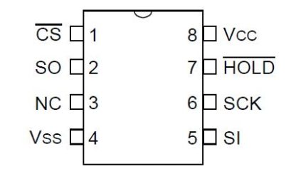
The following table shows the connections between the Vortex86 and the SRAM device.
| Vortex 86 Pin name | SRAM pin name |
| GPIO_P3[1]/SPI_CLK | SCK |
| GPIO_P3[2]/SPI_DO | SI |
| GPIO_P3[3]/SPI_DI | SO |
| GPIO_P2[0] | CS# |
For this example GPIO port 2 bit 0 has been allocated as the chip select pin but this can be any available GPIO signal.
Vortex86 SPI registers
There are 6 registers associated with the external SPI interface:-
| IO Address | Register Name |
| BA+08h | External SPI output data register |
| BA+09h | External SPI input data register |
| BA+0Ah | External SPI control register |
| BA+0Bh | External SPI status register |
| BA+0Ch | External SPI chip select register |
| BA+0Dh | External SPI error status register |
BA is the Base Address which is a programmable address stored in another register located at NorthBridge PCI configuration address 40h.
| Bit | Description |
| 31-4 | SPI base address |
| 03-Feb | Reserved |
| 1 | Memory or IO space |
| 0 | SPI base address enabled when set. |
Normally the Base address is set to FC08h. The following code example will allow this value to be computed rather than hard coded.
Example DOS program
#include <dos.h>
#include <stdio.h>
typedef unsigned char byte;
#define PCI_ADDRESS 0xcf8
#define PCI_DATA 0xcfc
#define PORT_2_DATA 0x7A
#define PORT_2_DIR 0x9A
// 32 bit operations
#define OPERAND32 asm db 66h
// prototypes
void outport32(unsigned long, unsigned long);
unsigned long inport32(unsigned long);
//———————————————————–
void main (void)
{
unsigned long SPI_reg_addr;
SPI_reg_addr=inport32(0x80000040) & 0x0000FFFFL; // read address from BADDR
if ((SPI_reg_addr & 0x1)==0)
{
printf(“SPI not enabled\n\r”);
return;
}
// show address type
if (SPI_reg_addr & 00000002L)
printf(“Address in memory space\n\r”);
else
printf(“Address in IO space\n\r”);
printf(“SPI reg Address = %04X\n\r”,SPI_reg_addr);
SPI_reg_addr &= 0x0000ffff0L;
SPI_reg_addr += 8; // for external SPI
printf(“Extern SPI base address = %04X\n\r”,SPI_reg_addr);
} // end of main
//———————————————————–
void outport32(unsigned long Address, unsigned long Data)
{
asm mov dx,PCI_ADDRESS
OPERAND32
asm mov ax,Address
OPERAND32
asm out dx,ax
asm mov dx,PCI_DATA
OPERAND32
asm mov ax,Data
OPERAND32
asm out dx,ax
}
//———————————————————–
unsigned long inport32(unsigned long Address)
{
long int Value;
asm mov dx,PCI_ADDRESS
OPERAND32
asm mov ax,Address
OPERAND32
asm out dx,ax
asm mov dx,PCI_DATA
OPERAND32
asm in ax,dx
OPERAND32
asm mov Value,ax
return Value;
}
//———————————————————–
The following tables detail the SPI registers:-
External SPI output data register – BASE_ADDR+08h
| BIT | Name | Attribute | Description |
| 7-0 | OUTDAT | WO | Write – Data output to SPI |
External SPI input data register – BASE_ADDR+09h
| BIT | Name | Attribute | Description |
| 7-0 | INDAT | R/W | Write – Preload data from SPI Read – Read data from register |
External SPI control register – BASE_ADDR+0Ah – Reset value = 15h
| BIT | Name | Attribute | Description |
| 07-May | RSD | RO | Reserved |
| 4 | FIEN | R/W | FIFO mode enabled when set |
| 3-0 | CKDIV | R/W | SPI clock divider=DRAM CLK/(2 * CKDIV) |
External SPI status register – BASE_ADDR+0Bh – Reset value = 10h
| BIT | Name | Attribute | Description |
| 7 | BUSY | RO | Set if controller busy |
| 6 | FIFU | RO | Set if FIFO full |
| 5 | IDR | RO | Set if input data ready |
| 4 | OCD | RO | Set if output complete / FIFO empty |
| 3-0 | RSVD | RO | Reserved |
External SPI chip select register – BASE_ADDR+0Ch – Reset value = 01h
This register will not be used in this example as the chip select will use a GPIO pin rather than the dedicated SPI_CS# controlled by this register.
| BIT | Name | Attribute | Description |
| 07-Jan | RSVD | RO | Reserved |
| 0 | CS | R/W | 0:CS# low 1:CS# high |
External SPI error status register – BASE_ADDR+0dh – Reset value = 00h
| BIT | Name | Attribute | Description |
| 07-May | RSVD | RO | Reserved |
| 4 | WCTE | R/WC | A write attempted to external SPI control register when controller was busy. Write ‘1’ to clear |
| 3 | DOLE | R/WC | Input data overlap Write ‘1’ to clear |
| 2 | FIURE | R/WC | FIFO under-run Write ‘1’ to clear |
| 1 | FIORE | R/WC | FIFO over-run Write ‘1’ to clear |
| 0 | RSVD | RO | Reserved |
23K640 SRAM device SPI commands:-
For simplicity this example will simply read and write a single byte in SRAM at location zero.
Write sequence:
– chip select low
– send write instruction – 02h
– send 16-bit address msb,lsb
– send data
– chip select high to terminate the operation
Read sequence:
– chip select low
– send read instruction – 03h
– send 16-bit address msb,lsb
– receive data
– chip select high to terminate the operation
To write a byte to the SPI the function simply needs to perform an IO write to the External SPI output data register. Before continuting the function needs to read the External SPI status register and wait until the interface is not busy and the ‘output complete bit’ is set.
To read a byte from the SPI the function needs to perform an IO write with any value to the External SPI input data register which causes the SPI to preload the register with data from the SPI device. The function needs to read the External SPI status register and wait until the interface is not busy and the ‘input data ready’ bit is set, then the data can be read back from the External SPI input data register.
Full source code
#include <dos.h>
#include <stdio.h>
typedef unsigned char byte;
#define PCI_ADDRESS 0xcf8
#define PCI_DATA 0xcfc
#define PORT_2_DATA 0x7A
#define PORT_2_DIR 0x9A
// 32 bit operations
#define OPERAND32 asm db 66h
// prototypes
void outport32 (unsigned long, unsigned long);
unsigned long inport32(unsigned long);
void write_sram(int, byte);
byte read_sram(int);
void wait_SPI_output_complete(void);
void wait_SPI_data_ready(void);
// global variables
unsigned long SPI_reg_addr;
void main (void)
{
byte SRAM_Data;
unsigned long Value;
int sb_val;
SPI_reg_addr=inport32(0x80000040) & 0x0000FFFFL; // read address from BADDR
if ((SPI_reg_addr & 0x1)==0)
{
printf(“SPI not enabled\n\r”);
return;
}
// show address type
if (SPI_reg_addr & 00000002L)
printf(“Address in memory space\n\r”);
else
printf(“Address in IO space\n\r”);
printf(“SPI reg Address = %04X\n\r”,SPI_reg_addr);
SPI_reg_addr &= 0x0000ffff0L;
SPI_reg_addr += 8; // for external SPI
printf(“Extern SPI base address = %04X\n\r”,SPI_reg_addr);
Value=inport32(0x800038c0);
printf(“GPIO setting = %X\n\r”,Value);
outport32(0x800038c0,Value | 0x00000001L);
Value=inportb(SPI_reg_addr+3);
printf(“SPI status reg = %X\n\r”,Value);
// set up the chip select on GPIO 2 pin 1
outportb(PORT_2_DIR,0x1); // bit 0 is output
write_sram(0x0,0x55);
printf(“Data read = %x\n\r”,read_sram(0));
write_sram(0x0,0xaa);
printf(“Data read = %x\n\r”,read_sram(0));
} // end of main
//———————————————————–
// Functions
//———————————————————–
void write_sram(int Address,byte Data)
{
byte msb, lsb, tmp;
// split the address into 2 bytes
lsb = Address & 0xff;
Address = Address >> 8;
msb = Address & 0xff;
outportb(PORT_2_DATA,0); // cs low
outportb(SPI_reg_addr,0x02); // issue write instruction
wait_SPI_output_complete();
outportb(SPI_reg_addr,msb); // address_msb
wait_SPI_output_complete();
outportb(SPI_reg_addr,lsb); // address_lsb
wait_SPI_output_complete();
outportb(SPI_reg_addr,Data); // data to write
wait_SPI_output_complete();
outportb(PORT_2_DATA,1); // cs high
}
//———————————————————–
byte read_sram(int Address)
{
byte msb, lsb, Data;
// split the address into 2 bytes
lsb = Address & 0xff;
Address = Address >> 8;
msb = Address & 0xff;
outportb(PORT_2_DATA,0); // cs low
outportb(SPI_reg_addr,0x03); // issue read instruction
wait_SPI_output_complete();
outportb(SPI_reg_addr,msb); // address_msb
wait_SPI_output_complete();
outportb(SPI_reg_addr,lsb); // address_lsb
wait_SPI_output_complete();
outportb(SPI_reg_addr+1,0×00); // preload data from SPI
wait_SPI_data_ready();
Data=inportb(SPI_reg_addr+1); // read in data
outportb(PORT_2_DATA,1); // cs high
return Data;
}
//———————————————————–
void wait_SPI_output_complete(void)
{
byte Value,Busy,Complete;
while (1)
{
Value = inportb(SPI_reg_addr+3);
Busy = Value & 0x80;
Complete = Value & 0x10;
if (Complete==0x10 && Busy==0) return;
}
}
//———————————————————–
void wait_SPI_data_ready(void)
{
// reads the stsatus register, ANDs the result with the mask and teturns 1 or zero
// bits 0-3 reserved
// bit 4 = output complete/FIFO empty when set
// bit 5 = input data ready when set.
// bit 6 = FIFO full
// bit 7 = Busy
byte Value,Busy,InputReady;
while (1)
{
Value = inportb(SPI_reg_addr+3);
Busy = Value & 0x80;
InputReady = Value & 0x20;
if (InputReady==0x20 && Busy==0) return;
}
}
//———————————————————–
void outport32(unsigned long Address, unsigned long Data)
{
asm mov dx,PCI_ADDRESS
OPERAND32
asm mov ax,Address
OPERAND32
asm out dx,ax
asm mov dx,PCI_DATA
OPERAND32
asm mov ax,Data
OPERAND32
asm out dx,ax
}
//———————————————————–
unsigned long inport32(unsigned long Address)
{
long int Value;
asm mov dx,PCI_ADDRESS
OPERAND32
asm mov ax,Address
OPERAND32
asm out dx,ax
asm mov dx,PCI_DATA
OPERAND32
asm in ax,dx
OPERAND32
asm mov Value,ax
return Value;
}
//———————————————————–
Disclaimer
All information contained in this application note is believed to be accurate and reliable. However, DSL Ltd assumes no responsibility for its use. Since conditions of product use are outside our control, we make no warranties express or implied in relation thereto. We therefore cannot accept any liability in connection with any use of this information. Nothing herein is to be taken as a license to operate under or recommendation to infringe any patents.
Whilst every effort has been made to ensure that this document is correct; errors can occur. If you find any errors or omissions please let us know so that we can put them right.